Technique Could Check Integrity of Computer Chips and Detect Tampering
Complete the form below to unlock access to ALL audio articles.
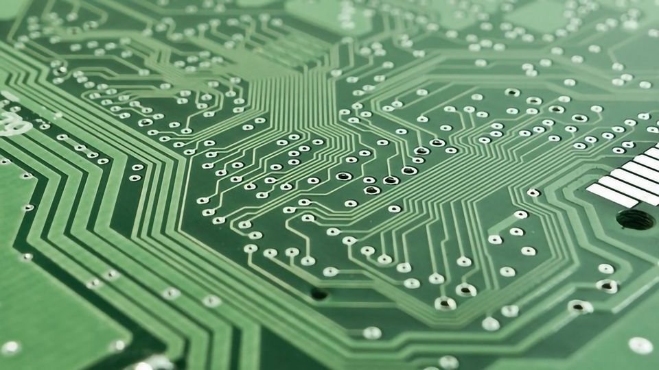
Guaranteeing that computer chips, that can consist of billions of interconnected transistors, are manufactured without defects is a challenge. But how to determine if a chip is compromised? Now a technique co-developed by researchers at the Paul Scherer Institut in Switzerland and researchers at the USC Viterbi School of Engineering would allow companies and other organizations to non-destructively scan chips to ensure that they haven’t been altered and that they are manufactured to design specifications without error.
Hardware security is a critical issue. Anthony F. J. Levi, Department Chair of the Ming Hsieh Department of Electrical Engineering-Electrophysics, co- author of the study, Three-dimensional imaging of integrated circuits with macro- to nanoscale zoom” published in Nature Electronics, says that “the supply chain for advanced electronics is susceptible.”
With this new method, it is possible to validate the integrity of computer chips using x-rays.
Called ptychographic x-ray laminography, the technique utilizes x-rays from a synchrotron to illuminate a small region of a rotating chip at an angle of 61 degrees (with respect to the normal of the chip plane). The resulting diffraction patterns are measured with a photon-counting detector array. The data are then used to generate high-resolution slice images of the chip, from which 3-D renderings are created.
Once the 3-D image is generated, it can be compared with the original design as a type of forensics to help companies or organizations that are looking to ensure chips are manufactured correctly and meet design specifications.
The researchers indicate that chips have signature features, so it is possible to tell how and where they were manufactured.
In addition, this process allows for reverse engineering of circuit designs without destroying the chip.
Levi says, “The majority of a chip’s intelligence is how it is wired. It is like the connectome of a brain.
By viewing a chip in detail, you can non-destructively figure out what it does. With this technology, hiding intellectual property in a chip is over.”
Levi imagines that the technology could one day contribute to a certification process to ensure the integrity of chips that are inserted into a computer or in communication hardware used by global businesses and governments.
The next steps are to continue to improve imaging speed and resolution and to further improve x-ray microscope performance.
Reference
Mirko Holler, Michal Odstrcil, Manuel Guizar-Sicairos, Maxime Lebugle, Elisabeth Müller, Simone Finizio, Gemma Tinti, Christian David, Joshua Zusman, Walter Unglaub, Oliver Bunk, Jörg Raabe, A. F. J. Levi, Gabriel Aeppli. Three-dimensional imaging of integrated circuits with macro- to nanoscale zoom. Nature Electronics, 2019; DOI: 10.1038/s41928-019-0309-z.
This article has been republished from the following materials. Note: material may have been edited for length and content. For further information, please contact the cited source.

