

Breaking Constraints With Ultracompact Metalens Microscopy
Complete the form below to unlock access to ALL audio articles.
The pursuit of ever-higher imaging resolution in microscopy is coupled with growing demands for compact portability and high throughput. While imaging performance has improved, conventional microscopes still suffer from the bulky, heavy elements and architectures associated with refractive optics. Metalenses offer a solution: they're ultrathin, ultralight, and flat, and benefit from lots of recent research that has improved their efficiency, FOV, and polarization functionalities.
According to Tao Li, professor of engineering and applied sciences at Nanjing University, "An ultra-compact metalens for imaging will miniaturize and even revolutionize conventional optical devices." Despite all the ongoing work to improve metalenses, most research groups are using them as a substitute for conventional refractive lenses in conventional optical settings. For metalenses to move toward real-world application, it's important to learn how to integrate metalenses into ultracompact optical devices.
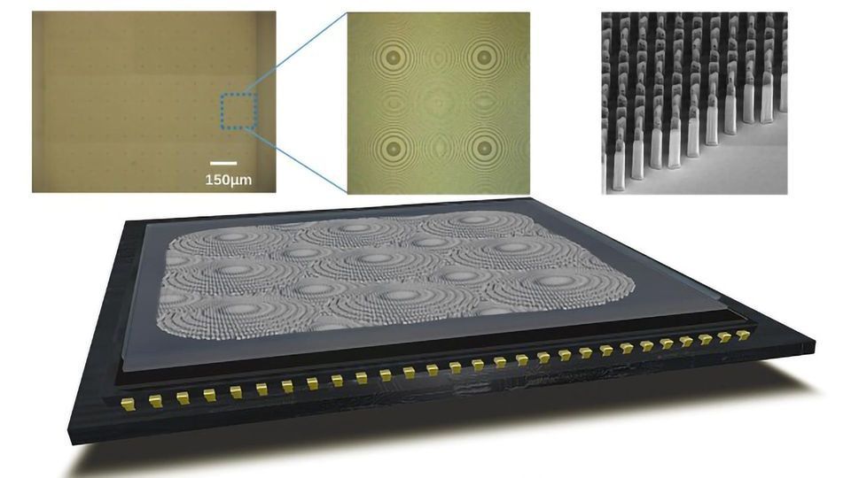
In pursuit of a compact integrated microscope system, Li's team mounted a metalens on a CMOS image sensor to create a prototype of a coin-sized imaging device. As reported in Advanced Photonics, their metalens-integrated imaging device (MIID) exhibits an ultracompact architecture with a working imaging distance in the hundreds of micrometers. Using a simple image-stitching process, they are able to obtain wide-field microscope imaging with large FOV and high resolution.
Pocket microscope system
The MIID prototype involves a millimeter-sized silicon metalens in a well-designed array of 6x6. Despite the integration of multiple lenses, imaging distance remains relatively small (~500 μm) because each single lens is sized about 200 μm. According to the authors, it can be extended to centimeter scale to cover the whole CMOS sensor.
The metalens array, which is a polarization multiplexer, has two different phase profiles corresponding to two circular light polarizations. According to Li, this arrangement ensures the elimination of blind areas.
The authors hope that the new MIID prototype heralds a new era of the pocket microscope system. They acknowledge that the imaging performance needs improvement and suggest a variety of approaches, such as adopting low-loss materials like GaN and SiN. They anticipate continuing advances in microscopy based on meta-technology in the future.
Reference
Li T, Li H, Gao S, et al. Metalens-integrated compact imaging devices for wide-field microscopy. AP. 2020;2(6):066004. doi:10.1117/1.AP.2.6.066004
This article has been republished from the following materials. Note: material may have been edited for length and content. For further information, please contact the cited source.

